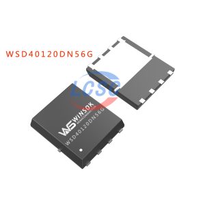
Currently, SGT process technology has been widely applied in WINSOK‘s mid- and low-voltage power MOSFET products with a “G” suffix in their product model numbers, such as WSD40120DN56G and WSF15N10G. The resistance of a MOSFET can be further reduced by decreasing the electric field of the MOSFET.
The SGT process has attracted increasing attention from manufacturers. SGT process technology is the leading technology in the field of medium and low voltage MOSFETs. The manufacturers with the best SGT technology are international power semiconductor factories, such as Infineon.
In the following, I will provide a brief introduction to the SGT process MOSFET and discuss its advantages.
Although IGBTs are currently very popular, MOSFETs still dominate a significant portion of the market. This is true across various sectors, including consumer electronics, household appliances, embedded systems, and industrial fields. Therefore, many manufacturers are continuing to increase their investment in the research and development of new technologies in MOSFETs, such as WINSOK.
There are four categories Mosfets: planar MOSFETs, trench MOSFETs, SGT process (Shielded Gate Transistor) MOSFETs, and Superjunction MOSFETs (SJ-MOSFETs). Planar MOSFETs are commonly used.Trench MOSFETs are primarily utilized in low-voltage (100V) applications. SGT process MOSFETs are primarily used in medium voltage (200V) applications, while SJ-MOSFETs are primarily used in high voltage (600V-800V) applications.

Compared to the conventional trench process, the SGT process has many advantages. Firstly, the SGT process is simpler, resulting in lower switching loss, smaller junction capacitance, and a narrower Miller platform. Secondly, the SGT process is 3-5 times deeper than the trench process. SGT can utilize a larger volume of silicon epitaxial volume laterally to block voltage, resulting in the internal resistance of SGT being approximately 2 times lower than that of an ordinary MOSFET. Additionally, SGT MOSFETs have a deeper trench depth, allowing for more silicon volume to be used in absorbing EAS energy. So, SGT can perform equally or even better in Avalanche. Last but not least, under the same specifications, the chip area can be smaller and more cost-effective.
With the development of 5G, AI, electric vehicle(EV), and other application markets, the demand for high-end MOSFETs is growing rapidly. Many power semiconductor manufacturers are now focusing on developing the SGT process MOSFET, which offers high power density and low internal resistance.
