Exposed Pad Soldering and PCB Heat Management Guide
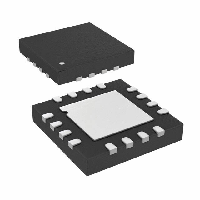
With modern electronic devices getting smaller, effective thermal management is more critical than ever. High-density PCB designs often face serious heat dissipation challenges, especially when using QFN (Quad Flat No-lead) packages. Unlike traditional leaded packages, QFNs rely on their exposed pad for both electrical grounding and heat dissipation.
For high-power chips, thermal performance affects circuit stability and lifespan. A poorly designed heat dissipation path may cause partial overheating, leading to device failure. Optimizing the design of exposed pads and soldering processes can significantly improve heat dissipation efficiency.
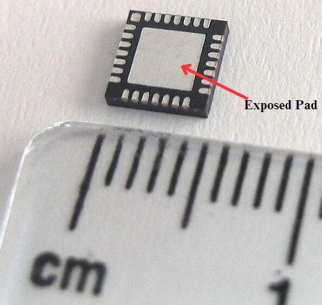
What Is an Exposed Pad?
The exposed pad, also known as the thermal landing, is part of the chip’s lead frame. It serves dual purposes:
- Thermal conduction: It provides a direct path for heat transfer from the die to the PCB copper layers.
- Electrical connection: It helps with grounding and reduces electrical noise.
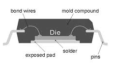
The pad forms a low–thermal resistance in the heat conduction path by directly connecting the silicon die inside the chip to the external PCB copper foil.
The merits of this structure:
- Low parasitic inductance, making it suitable for high-frequency applications.
- Excellent thermal performance lowers the overall thermal resistance of the chip.
However, exposed pad soldering requires precise control over voids, solder paste volume, and via design to ensure reliable performance.
Key Challenges in Exposed Pad Soldering
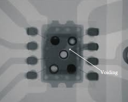
Solder Voids and Cold Solder
- If gas is trapped during soldering, voids form within the solder joint, reducing thermal and electrical conductivity.
Component Floating
- Excessive solder paste can lift the chip off the PCB, affecting quality of the surrounding pads.

Incorrect Via Design
- Poorly designed vias can cause solder leakage, leading to poor bonding and heat dissipation inefficiencies.
How to Optimize Exposed Pad Design for Better Heat Dissipation in Thermal Management Strategy?
Copper Pad Size Optimization
- Ensure that the PCB pad is slightly larger than the chip’s exposed pad to maximize heat transfer.
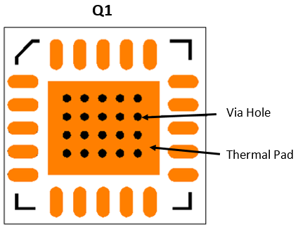
Thermal Via Design
- Use 13-mil diameter Vias within the solder pad by following the manufacturer’s guidelines, which normally provides reliable data.
- Use 25-mil diameter Vias outside the solder area to provide additional heat dissipation path.
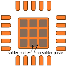
Segmented Solder Paste Application
- Instead of covering the entire pad, divide it into smaller sections (e.g., 9-segment pattern) covering about 60% of the area. This helps gases escape and prevents excessive solder buildup.
Advanced Copper-Core PCB: A Breakthrough in Thermal Management
Traditional PCBs rely on standard copper or aluminum substrates for heat dissipation. However, these materials have limitations due to the thermal resistance of their insulating layers. LCSC introduces a cutting-edge Direct Heatsink Copper-Cored PCB, designed to enhance thermal performance for high-power applications.
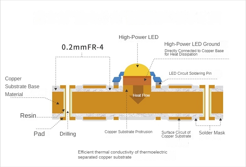
How Does the Direct Heatsink Copper-Cored PCB Work?
- Working Principle: Unlike conventional designs, this technology separates electrical and thermal pathways by using a dedicated heat-conducting protrusion to transfer heat directly to the copper core.
- Heat conduction efficiency: With a thermal conductivity of 380 W/m·K, this new technology vastly outperforms traditional PCBs (which typically range from 1–18 W/m·K).
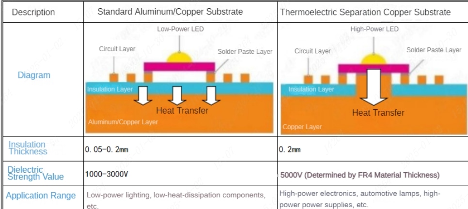
| Comparison | Single-Sided Copper/Aluminum Substrate | Thermoelectric Separation Copper Substrate |
| Heat Conduction Mechanism | Heat must pass through the insulating layer (thermal conductivity of only 1–18 W/m·K) before reaching the copper or aluminum base. The insulating layer limits overall heat dissipation efficiency. | Heat is directly transferred to the copper base through a thermal conduction protrusion, bypassing the insulating layer entirely, while FR4 material provides structural support. This design significantly enhances heat dissipation efficiency. |
| Summary | Due to the thermal limitations of the insulating layer, heat dissipation efficiency is low, making it difficult to meet the cooling demands of high-power chips. | Direct heat conduction maximizes the thermal advantages of the copper substrate, significantly improving thermal management for high-power chips. |
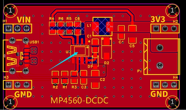
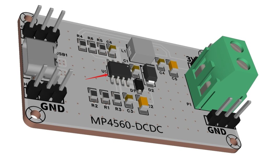
Case Study: Thermal Management Optimization for MP4560 DC-DC Converter
In an MP4560 buck converter design, the initial PCB used FR-4 material, which struggled to handle the high-frequency and high-current conditions. The poor heat dissipation affected performance and reliability in long-term operation.
To solve this problem, the design team used a thermoelectrically separated, double-sided copper substrate and added a specialized protrusion underneath the exposed pad on the bottom of the MP4560DN-LF-Z. The module’s thermal performance is effectively improved, resulting in a significant reduction in the surface temperature of the PCB. In addition, the heat from the module can be quickly transferred to the copper substrate and diffused, further improving the cooling efficiency.
After testing, the thermal efficiency of this design is significantly improved compared to the original solution. This thermal management method is not only applicable to the MP4560, but can also be extended to other high-power DC-DC converter designs. The use of a copper substrate and a proper thermal structure not only significantly improves circuit performance but also extends product life.
Some images are sourced online. Please contact us for removal if any copyright concerns arise.
Custom Cables: Save 50%+ Avg Cost By JST, Molex, TE Alternatives | Processing Fee Down to $1 Per Piece | No Minimum Order Quantity (MOQ) Required
PCB & PCBA: New Customer Get Coupons Up to $125 | 1 – 32 Layers From $2 /5pcs | PCB Assembly From $8 /5pcs
Front Panels: High-quality Front Panel Acrylic/PET | Front Panel Order Up to 30% Off | Membrane Switch Available Soon